Simple Clap Controlled Electronic Switch Circuit Diagram

This electronic switch allows you to control an electronic device by only clapping your hands twice. It is based on three integrated circuits; 741 Op-Amp, 555 timer, and 4013 dual D flip-flop.A 9V battery is ample to operate the circuit.

When you first clamp your hands, mic detects the sound and triggers the 555 timer via the operational amplifier. The timer stretches the signal and applies it to the clock input of the flip-flop. Because of the three state arrangement of the flip-flop , one more clamp is needed to change the output state.
 
 Clap Controlled Electronic Switch Circuit Diagram
 
 
Clap Controlled Electronic Switch Circuit DIagram
 
 Second clamp sets the flip-flop output to high and this forward biases the 2N2222 BJT. Relay closes so the device connected to the relay switches on. Same procedure applies for the opposite. When you clap your hands twice, relay closes and turns off the device connected to it.

R3 trimpot adjusts the sensitivity of the circuit. You should turn it till the room noise does not effect the switch operation.


    Components


IC1: 741 Op-Amp
IC2: 555 Timer
IC3: 4013 Dual D Flip-Flop
Q1: 2N2222 NPN Transistor
C1, C2, C3, C4: 0.1uF Ceramic Capacitor
C5: 47 uf Electrolytic Capacitor
R1, R2, R4, R5, R10: 10 KOhm
R6: 150 KOhm
R7, R9: 100 KOhm
R8: 1 MOhm
R11: 220 Ohm
R3: 100 KOhm Trimpot
B1: 9 Volt Battery,
K1: SPST Reed Relay 5 Volt DC Coil
MIC: Electret Microphone

Built a Soft-Action Mute Switch Circuit Diagram

This is the simple Soft-Action Mute Switch Circuit Diagram. This simple circuit is a line-level audio signal muting switch based on a soft-action power on/off process. When the S1 switch is closed, R4, C1 and Q4 JFET quietly ground the signal to be muted in between 100 to 200 ms and the RED indicator light goes on. When the S1 is opened the signal is released and the GREEN led goes on.

 Soft-Action Mute Switch Circuit Diagram


Built a Soft-Action Mute Switch Circuit Diagram


Potentiometer R2 must be set to the value twice of the transistor's cut-off voltage so the on/off transition times become approximately equal. R2 and D3 discharge C1 swiftly and mute the signal during the power down. In this process, the signal path should remain stable to below 1/3 of the normal supply voltage (In this example below +/-4). Then Q1 - 2N3819 finishes muting. 


Digital Sound activated Switch Circuit Diagram

This is an Electronic Digital Sound activated Switch Circuit Diagram. A sensitive electret microphone picks up the sound and feeds the signal to a two-stage amplifier circuit, consisting of Ula and Ulb. The amplified output of Ulb is fed ·to a voltage-doubler circuit (comprised of Dl, D2, C4, and C5). The output of the doubler is input to the gate of Ql. When the de voltage reaches the gate`s threshold level, Ql switches on, starting the recorder. Resistor R6 sets the circuit`s sensitivity and should be experimented with to obtain the optimum adjustment.

Digital Sound activated Switch Circuit Diagram


Simple Dual Trace Scope Switch Circuit Diagram

Simple Dual Trace Scope Switch Circuit Diagram. The switcher output goes to the single vertical input of the scope, and a sync line from one of the inputs is taken to the scope's external-sync input. Frequency response of the input amplifiers is 300 kHz over the range of the gain controls. With the gain controls wide open so no attenuation of the signal takes place, the frequency response is up to 1 MHz. 

 Simple Dual Trace Scope Switch Circuit Diagram


Simple Dual Trace Scope Switch Circuit Diagram

Simple Rf Power Switch Circuit Diagram

This is a Simple Rf Power Switch Circuit Diagram. This Rf power switch operates at 1. 7 MHz with a 50-V source and load. Its on loss is 0.2 dB and its off isolation is 30 dB. It provides 40-W PEP, 45 VrEAK and 0.9 APEAK· The control input can come from CMOS, TTL, LS, etc., to turn on Q1, which turns on Q2, a TMOS MTP3N35.

Simple Rf Power Switch Circuit Diagram


Simple Rf Power Switch Circuit Diagram

Simple Comparator with time out Circuit Diagram

This is a Simple Comparator with time out Circuit Diagram. The MC1422 is used as a comparator with input (Pin 5). The frequency of the pulses for the capability of a timing output pulse when the the values of R2 and Cl as shown is approx i-inverting input (Pin 6) is the non inverting mately 2 Hz, and the pulse width 0 ms.

Simple Comparator with time out Circuit Diagram


Simple Comparator with time out Circuit Diagram

Audio Operated Switch Circuit Diagram

This is a simple Audio or voice Operated Switch Circuit Diagram. The sound picked up by SPKRl, which acts as a microphone, is fed to transistor amplifier Ql. The output of Ql is applied across coupling transformer T1 and is used to drive the gate circuit of Triac TRl. TRl is used to lend a latching effect to the action of the relay.

Audio Operated Switch Circuit Diagram


Audio Operated Switch Circuit Diagram

Two-channel Audio/Video Switcher Circuit Diagram

This is a simple Two-channel Audio/Video Switcher Circuit Diagram. This circuit is a two-channel base band video switcher. Buffer amps Ul/Ql, U4/Q4, and associated components produce a buffered 75- video signal, which is routed to switching network K1/K2/K3. Relay K1 selects either of these two video amplifiers and feeds J7. K2 also routes the output of either video amplifier to K3, which passes the selected video channel to J8 or connects J9 to J8. U2 and J3 are audio amplifiers, which drive U7 and J8 (CD4053 analog switches) to route audio from J1 and J2 to either J14/J15, or J10/J11. Also, audio from J12/J13 can be routed to these jacks.

Two-channel Audio/Video Switcher Circuit Diagram


Two-channel Audio/Video Switcher Circuit Diagram

Simple Digital Switching Circuit Diagram

This is a Simple Digital Switching Circuit Diagram. This switching circuit acts like a bank of interlocked mechanical switches; pushing one of the buttons latches its corresponding output and unlatches a previously selected output. A pair of inverters forms a latch for each output. Pressing button Bl, for example, applies a positive pulse, via resistor diode DIB, to the input of the first output`s, OUT1, latch. 

 Simple Digital Switching Circuit Diagram

 
Simple Digital Switching Circuit Diagram

This positive pulse will set OUT1 high. Feedback locks OUTl`s pair of converters in this HIGH state. Meanwhile, the pulse will also pass through diode D1A to the differentiator that is formed by C and R2. The differentiator will shorten the pulse. The shortened pulse goes to all the latches and resets all of them, except the latch that sees the longer setting pulse. Obviously, if you press more than one button at once, more than one output will latch at once.

Differential Analog Switch Circuit Diagram

This is a simple Differential Analog Switch Circuit Diagram. The NPD5566 monolithic dual is used in a differential multiplex application where Rds(ON> should be closely matched) for the monolithic dual tracks at better than ±1% over wide temperature ranges (-25° C to +125° C), this makes it an unusual but ideal choice for an accurate multiplexer. This close tracking greatly reduces errors due to common-mode signals. 

Differential Analog Switch Circuit Diagram


Differential Analog Switch Circuit Diagram
 

Electronic Push-on Push-off Switch Circuit Diagram

This is a simple Electronic Push-on Push-off Switch Circuit Diagram. Transistors Ql and Q2 make up the flip-flop while Q3 drives a reed relay. When power is first applied to the circuit, Ql and Q3 are conducting and Q2 is cut off. Momentarily closing SI causes the flip-flop to switch states—Ql cuts off and Q2 conducts. When Q2 is conducting, its collector drops to around 0.6 volt. 

 Electronic Push-on Push-off Switch Circuit Diagram


Electronic Push-on Push-off Switch Circuit Diagram


That prevents base current from flowing into Q3 so it is cut off, de-energizing relay Kl. The flip-flop changes state every time SI is pressed. Capacitors Cl and C2 ensure that Ql is always the transistor that turns on when power is first applied to the circuit. When power is first applied to the basic flip-flop, the initial status is random—Ql and Q2 both try to conduct and, usually, the transistor with the higher gain will take control, reaching full conduction and cutting off the other one. 

However, differences in the values of the collector and coupling resistors will also influence the initial state at power-on. With C2 in the circuit, it and R4 form an R-C network that slightly delays the rise in Q2's base voltage. That gives Ql sufficient time to reach saturation and thus take control.

Electric Zero Voltage Switching Circuits Diagram

This is the Electric Zero Voltage Switching Circuits Diagram. These circuits are effective for lamp and heater loads. Some circuits driving reactive loads require integral cycling and zero-voltage switching-when an identical number of positive and negative half cycles of voltage are applied to the load during a power period. 

Electric Zero Voltage Switching Circuits Diagram


Electric Zero Voltage Switching Circuits Diagram

 The circuit, although not strictly a relay because of the three-terminal power connection, performs the integral cycle ZVS function when interfaced with the previous coil circuits. Fiber optics offers advantages in power control systems. Electrical signals do not flow along the nonconducting fiber, minimizing shock hazard to both operator and equipment. EMIIRFI pick up on the fiber is nonexistent-although high gain receiver circuits might require shielding, eliminating noise pick-up errors caused by sources along the cable route. 

Both ac and de power systems can be controlled by fiber optics using techniques sinillar to the optoisolator solid-state relay. Triac triggering is accomplished through the Cl06BX301, a low gate trigger current SCR, switching line voltage derived current to the triac gate via the full-wave rectifier bridge. The primary difference between fiber optics solid-state relay circuits and optoisolator circuits is the gain; photo currents are much smaller.

Simple Switch Debouncer With Auto Repeat Circuit Diagram

This is a Simple Switch Debouncer With Auto Repeat Circuit Diagram. This circuit produces an output pulse when SW1 (pushbutton) is depressed. It also becomes a hysteresis gate oscillator. Dl and R2 add asymmetry. The DBRT (delay before repeat time) is caused by the oscillator start-up conditions: CI has to change from zero to the upper gate threshold rather than to the lower threshold. The auto repeat time: Gate hysteresis « 1 V for 74HCT14 gate, DBRT= 0.7T (upper gate threshold hysteresis). Upper gate threshold 2.3 V for HCT14, Ri<

Switch Debouncer With Auto Repeat Circuit Diagram


Switch Debouncer With Auto Repeat Circuit Diagram

Simple 1 Mospower Fet analog Switch Circuit Diagram

This is a Simple 1 Mos-power Fet analog Switch Circuit Diagram. This circuit Using four diode in an array allows using only one MOSPOWER transistor for analog switching. The current flow is controlled by keeping the source-base connection of the MOSFET towards the load. 

 Simple 1 Mospower Fet analog Switch Circuit Diagram


Simple 1 Mospower Fet analog Switch Circuit Diagram

Be sure to use diodes capable of handling the load current and a transistor whose breakdown voltage specification exceeds the peak analog voltage anticipated. Operationally, by increasing the gate-to-source bias voltage, the MOSFET turns on. For applications other than either full-on or fulloff, care must be taken not to exceed the dissipation of the MOSPOWER transistor. A suitable heatsink cannot be overstressed in such applications.

Line Operated Power outage Light Circuit Diagram

This is a simple Line Operated Power outage Light Circuit Diagram. This circuit provides emergency lighting during a power outage. The photo transistor should be positioned to maximize coupling of both neon light and ambient light into the pellet, without allowing self-illumination from the 6-V lamp. Many circuits of this type also use line voltage to charge the battery. 

 Line Operated Power outage Light Circuit Diagram


Line Operated Power outage Light Circuit Diagram

Electric Voltage Comparator Circuit Diagram

This is simple Electric Voltage Comparator Circuit Diagram. An op amp is used as a comparator and a sink for LED current.

 Electric Voltage Comparator Circuit Diagram


Electric Voltage Comparator Circuit Diagram


 The output voltage of the amplifier changes about 1.4 V depending on the direction of the current. Only one transistor is on at any time. Maximum LED current is limited to 25 mA by over current protection of the uA741.

If LEDs are not capable of carrying such a current or an alternative op amp is used and an additional resistor R^ is necessary.

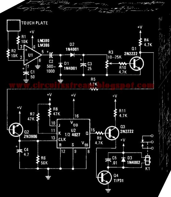
Electronic Touch Switch 1 Circuit Diagram

This is an Electronic Touch Switch 1 Circuit Diagram. This switch reacts to the touch of a finger to turn lights and/or appliances on or off. The device uses the human body as an antenna to pick up 60-Hz hum, which is applied to a metal plate by your finger. The signal is fed to the input of Ul, an LM380 audio-power amplifier. An LM386 should work as well. 
 

 Electronic Touch Switch 1 Circuit Diagram


 Electronic Touch Switch 1 Circuit Diagram
 
The 60-Hz output from the amplifier is rectified by Dl and D2, then filtered by C3. Potentiometer R3 sets the trigger voltage used to saturate Ql. When Ql turns on, the collector end of R4 goes almost to ground and provides the needed voltage to turn on Q2. Transistor Q2 turns on and clocks. 
 
The flip-flop is configured for toggle-mode operation, so its output switches states with each clock pulse. The 4027 (U2) is wired to toggle by tying the J and inputs high and the set and resets low. Transistor Q3 is connected to the Q output through the 4.7-KOhmhm resistor. Transistor Q3 drives Q4, the relay driver. Be sure that the load does not exceed the relay ratings.

Snubber Triggering scr series Circuit Diagram

This is a simple switching Snubber Triggering scr series Circuit Diagram. A simple snubber uses a small resistor (R) in series with a small capacitor (C). This combination can be used to suppress the rapid rise in voltage across a thyristor, preventing the erroneous turn-on of the thyristor; it does this by limiting the rate of rise in voltage (dV/dt) across the thyristor to a value which will not trigger it. Snubber circuit R2C2, as shown, might be necessary since Rl and Cl are tailored for optimized triggering and not for dV!dt protection. Fiber-optic pairs can be used with discrete SCRs to switch thousands of volts. 

 Snubber Triggering scr series Circuit Diagram


Snubber Triggering scr series Circuit Diagram

A photon coupler with a transistor output will limit the trigger-pulse amplitude and rise time because of CTR and saturation effects. Using the HllCl, the rise time of the input pulse to the photon coupler is not critical, and its amplitude is limited only by lite HllCl turn-on sensitivity. The load can also be connected to the cathode as illustrated in Fig. 67-3B.

Simple Shutdown Circuit Diagram II

This is a Simple Shutdown Circuit Diagram II. These modern devices have shutdown circuits that are designed to remove power from the device under power when the voltage rises above a predetermined threshold.This one blows a fuse to protect the device under power.


Simple Shutdown Circuit Diagram II


Simple Shutdown Circuit Diagram II

Simple Schmitt trigger III Circuit Diagram

We build 1st Simple Schmitt trigger Circuit Diagram and Simple Schmitt trigger II Circuit Diagram. Now we made to day Simple Schmitt trigger III Circuit Diagram. In this simple circuit the lower trigger point is fixed at % Vcc, but the upper trigger point is adjustable by means of Pin 5 from Vi Vcc to slightly less than Vcc. The Schmitt trigger will operate with input frequencies up to 50 kHz.

Simple Schmitt trigger III Circuit Diagram


Simple Schmitt trigger III Circuit Diagram


All updates in Your Inbox

Enter your email address:

Delivered by FeedBurner


Copyright @ 2013 Electronic Circuit Diagrams & Schematics.

Designed by AS & AS