Simple Latch Circuit Diagram

This is a Simple Latch Circuit Diagram project. Electronic latch circuits can be either active-high or active-low. The difference is determined by whether the operation of the latch circuit is triggered by HIGH or LOW signals on the inputs.

    Active-high circuit: Both inputs are normally tied to ground (LOW), and the latch is triggered by a momentary HIGH signal on either of the inputs.

    Active-low circuit: Both inputs are normally HIGH, and the latch is triggered by a momentary LOW signal on either input.

These two projects show you how to build simple active-high and active-low latch circuits using a 4001 quad 2-input NOR gate integrated circuit (IC) and a 4011 quad 2-input NAND gate IC. Both the Q and Q-bar outputs are used to drive LEDs so you can see the state of the latch, and both inputs are controlled by normally-open pushbuttons so that you can trigger the latch by momentarily pressing the buttons.

This is what the assembled active-high latch will look like when you are done:

Simple Latch Circuit Diagram


If you compare the schematic diagrams between these two projects, you’ll see that there are only these two differences between them:

    Gates: The active-high circuit uses a 4001 IC that contains NOR gates, while the active-low uses a 4011 IC, which contains NAND gates.

    Resistor and switch positions: The positions of R1 and R2 and SW1 and SW2 are reversed. In the active-high circuit, the resistors connect the two gate inputs to ground and the switches short the gate inputs to +6 V. In the active-low circuit, the resistors connect the gate inputs to +6 V and the switches short the gate inputs to ground.

Both of these circuits use simple pushbutton switches to provide the trigger inputs. However, you can easily imagine other sources for the trigger pulse. For example in a home alarm system, the SET-bar input in an active-low latch might come from a window switch that breaks contact when the window is open, and the RESET-bar input may come from a key lock on the alarm system’s control panel.

Once you have completed the second project, your assembled active-low latch will look like this:


A latch with a SET and RESET input is often called an SR latch. The term RS latch is also used.

In some cases, you may need a latch in which one of the inputs is active-high and the other is active-low. For example in the alarm system described in the previous paragraph, the key lock may send a HIGH signal when the alarm should be reset. Thus, the SET-bar input for the alarm latch is active-low, but the RESET input is active high.

You can easily accomplish that by adding an inverter to one of the inputs. Here, I’ve used NAND gates to create an active-low latch, but I’ve added a NOT gate to invert the RESET input. Thus, the SET-bar input of this inverter is active-low, and the RESET input is active-high.

Simple Latch Circuit Diagram


Sourced by: dummies / Doug Lowe

Arduino Uno Board - DC Motor Starter Circuit

Motor starter reduces the load, torque and current surge of a motor during startup. On starting, the motor takes more than five times the normal running current. This overheats the motor’s armature winding and creates a sudden voltage dip in the power supply, which can be avoided by using a motor starter. There are many types of motor starters. Here we describe an electronic DC motor starter using Arduino Uno board. This circuit controls both soft-start and soft-stop timings through pulse-width modulation (PWM).

Circuit and working

Circuit diagram of the DC motor soft-starter is shown in Fig. 1. In addition to Arduino Uno board (Board1), it uses PIC817 optocoupler (IC1), p-channel IRF9530 MOSFET (T1), 1N4007 rectifier diode (D1), 12V DC motor (M1) for testing, bi-colour LED (LED1) and a few other components.

Arduino Uno Board - DC Motor Starter
Fig. 1: Circuit diagram of DC motor starter using Arduino Uno

Arduino Uno board is an important part of the circuit that generates PWM signals. Pushbuttons (S1 and S2) are used to soft-start and soft-stop the motor. The bi-colour LED indicates whether the motor is in soft-start or soft-stop mode.
Soft-start

When the circuit is switched on, the motor is at rest and LED1 off. When push button S1 is pressed momentarily, the voltage across the motor increases gradually and attains maximum voltage after the predetermined soft-start timing. So the motor first starts at a slow speed. In this state, LED1 emits green light. After the soft-start time, i.e., in running condition, LED1 emits orange light, indicating that the motor is running at the rated speed.
Soft-stop

If pushbutton S2 is pressed momentarily while the motor is running at the rated speed, the voltage across the motor decreases gradually and becomes zero after the soft-stop time. So the motor speed also decreases gradually and it finally stops after the soft-stop time. In this state, LED1 emits red colour. After the soft-stop time, LED1 doesn’t glow, indicating that the motor is at rest.

Arduino Uno is programmed such that if switch S1 or S2 is pressed more than once before the timing ends, it executes only once. This prevents the motor from restarting suddenly.
The circuit is isolated by an optocoupler (IC1) so that any disturbance in the motor power supply doesn’t affect the Arduino Uno board. The freewheeling diode (D1) gives additional protection over induced voltage when the motor is turned off.


The circuit’s operation is controlled using the software program loaded into the internal memory of Arduino Uno board. The program (softs.ino) is written in Arduino programming language sketch. Arduino IDE is used to compile and upload the program to the Arduino board.

Construction and testing

A PCB layout of the DC motor soft-starter is shown in Fig. 2 and its components layout in Fig. 3. After assembling the circuit on a PCB, connect CON2 to Arduino Uno board through external male-to-male jumper wires. After uploading the code to Board1, enclose the assembled PCB along with Board1 in a suitable plastic box.

The circuit works off the 5V USB power supply used for Arduino Uno board. Regulated 12V power supply is used to operate the DC motor.


Fig. 2: PCB layout of the DC motor starter using Arduino Uno

Fig. 3: Components layout for the PCB


The circuit can be converted into an AC motor soft-starter by using thyristors in place of MOSFET T1. It can be used along with device control projects. Additional protection and closed-loop control can be included, if required. Different timings and PWM values can be set for both soft-start and soft-stop.


Sourced By: Streampowers

Introduction to Amplifier (Rise)

Amplification is the method of increasing the amplitude of a AC signal current or voltage such as audio signal for sound or video signal for a television picture. The amplifier allows a small input signal to control a bigger amount of power in the output circuit. The output signal is a replica of the original input signal but has higher amplitude.

Amplification is necessary as in most applications, the signal is weak to be used directly. For example, an audio output of 1mV from a microphone is unable to drive a loud speaker which requires a few volts to operate. Hence, the signal require to be amplified to a few volts before it can be fed in to the loud speaker.

NP N Transistor Circuit Configurations
An example of different type of transistor configurations in the circuit.


(1) The common emitter(CE) circuit makes use of emitter as its common electrode. The input signal is applied to the base and the amplified output is taken from the collector. This is the usually use because it's the best combination of current gain & voltage gain.

(2) The common base (CB) circuit makes use of base as its common electrode. The input signal is applied to the emitter & the amplified output is taken from the collector. The comparatively high emitter current compared to the base current ends in low input impedance value. For this reason, the CB circuit is never used.

(3) The common collector (CC) circuit makes use of collector as its common electrode. The input signal is applied to the base & the amplified output is taken from the emitter. This circuit is also called an emitter follower. This name means that the output signal voltage at the emitter follows the input signal at the base with the same phase but less amplitude. The voltage gain is less than one & is usually used for impedance matching. It's high input at the base as a load for the earlier circuit & low output impedance at the emitter as a signal source for the next circuit.

Classes

They can be classified in to classes A, B, C & AB. They are defined based on the percent of the cycle of input signal that can produce output current.

In Class A, the output current flows for the full cycle of 360 degree of input signal. The distortion is the lowest with around 5% to 10% &an efficiency of 20% to 40%. In general, most tiny signal operate class A

In Class C, the output current flows for less than half of the input cycle. Typical operation is 120 degree of input current in the coursework of the positive half cycle of the input current. This class has an efficiency of 80% but has the highest distortion. This class is usually used for RF amplification with a tuned circuit in the output.

In Class B, the output current flows for half of the input cycle which is around 180 degree. Class B operation lies between class A & class C. Classes B are usually connected in pairs & in such a circuit called push-pull amplifier. The push pull is often used for audio power output to a loud speaker.

In Class AB, it offers a compromise between the low distortion of class A & the higher power of class B. It is usually used for push pull audio power amplifiers.

10 W Audio Amplifier Circuit Diagram

This design is based on the 18 Watt Audio Amplifier, and was developed mainly to satisfy the requests of correspondents unable to locate the TLE2141C chip. It uses the widespread NE5532 Dual IC but, obviously, its power output will be comprised in the 9.5 - 11.5W range, as the supply rails cannot exceed ±18V.

10 W Audio Amplifier Circuit Diagram

10 W Audio Amplifier Circuit Diagram

As amplifiers of this kind are frequently used to drive small loudspeaker cabinets, the bass frequency range is rather sacrificed. Therefore a bass-boost control was inserted in the feedback loop of the amplifier, in order to overcome this problem without quality losses. The bass lift curve can reach a maximum of +16.4dB @ 50Hz. In any case, even when the bass control is rotated fully counterclockwise, the amplifier frequency response shows a gentle raising curve: +0.8dB @ 400Hz, +4.7dB @ 100Hz and +6dB @ 50Hz (referred to 1KHz).

Notes:

    Can be directly connected to CD players, tuners and tape recorders.
    Schematic shows left channel only, but C3, C4, IC1 and the power supply are common to both channels.
    Numbers in parentheses show IC1 right channel pin connections.
    A log type for P2 will ensure a more linear regulation of bass-boost.
    Do not exceed 18 + 18V supply.
    Q3 and Q4 must be mounted on heatsink.
    D1 must be in thermal contact with Q1.
    Quiescent current (best measured with an Avo-meter in series with Q3 Emitter) is not critical.
    Set the volume control to the minimum and R3 to its minimum resistance.
    Power-on the circuit and adjust R3 to read a current drawing of about 20 to 25mA.
    Wait about 15 minutes, watch if the current is varying and readjust if necessary.
    A correct grounding is very important to eliminate hum and ground loops. Connect to the same point the ground sides of J1, P1, C2, C3 &C4. Connect C9 to the output ground.
    Then connect separately the input and output grounds to the power supply ground.

Parts:

P1_________________22K   Log.Potentiometer (Dual-gang for stereo)
P2________________100K   Log.Potentiometer (Dual-gang for stereo)
R1________________820R   1/4W Resistor
R2,R4,R8____________4K7  1/4W Resistors
R3________________500R   1/2W Trimmer Cermet
R5_________________82K   1/4W Resistor
R6,R7______________47K   1/4W Resistors
R9_________________10R   1/2W Resistor
R10__________________R22   4W Resistor (wirewound)

C1,C8_____________470nF   63V Polyester Capacitor
C2,C5_____________100µF   25V Electrolytic Capacitors
C3,C4_____________470µF   25V Electrolytic Capacitors
C6_________________47pF   63V Ceramic or Polystyrene Capacitor
C7_________________10nF   63V Polyester Capacitor
C9________________100nF   63V Polyester Capacitor

D1______________1N4148    75V 150mA Diode

IC1_____________NE5532    Low noise Dual Op-amp

Q1_______________BC547B   45V 100mA NPN Transistor
Q2_______________BC557B   45V 100mA PNP Transistor
Q3_______________TIP42A   60V 6A    PNP Transistor
Q4_______________TIP41A   60V 6A    NPN Transistor

J1__________________RCA audio input socket

Power supply parts:

R11_________________1K5  1/4W Resistor

C10,C11__________4700µF   25V Electrolytic Capacitors

D2________________100V 4A Diode bridge
D3________________5mm. Red LED

T1________________220V Primary, 12 + 12V Secondary 24-30VA Mains transformer

PL1_______________Male Mains plug

SW1_______________SPST Mains switch


Technical data:

Output power:
    10 Watt RMS into 8 Ohm (1KHz sinewave)
Sensitivity:
    115 to 180mV input for 10W output (depending on P2 control position)
Frequency response:
    See Comments above
Total harmonic distortion @ 1KHz:
    0.1W 0.009% 1W 0.004% 10W 0.005%
Total harmonic distortion @ 100Hz:
    0.1W 0.009% 1W 0.007% 10W 0.012%
Total harmonic distortion @ 10KHz:
    0.1W 0.056% 1W 0.01% 10W 0.018%
Total harmonic distortion @ 100Hz and full boost:
    1W 0.015% 10W 0.03%
Max. bass-boost referred to 1KHz:
    400Hz = +5dB; 200Hz = +7.3dB; 100Hz = +12dB; 50Hz = +16.4dB; 30Hz = +13.3dB
Unconditionally stable on capacitive loads


18W Car Stereo Amplifier Circuit Diagram

This automobile stereo amplifier project is a class AB audio power amplifier using the Hitachi HA13118 module. It not only can be used in automobile application but also in any transportable or home amplifier process. It is simple to construct & has a maximum of outside parts. The module has a high power output from a low voltage supply using the bridge tied load system, & a high gain of 55dB.

This project will be useful in applications where the input signal is a low level, without requiring the use of a separate pre-amplifier. This IC module has a built in surge protection circuit, thermal shutdown circuit, ground fault protection circuit & power supply fault protection circuit making it reliable.
The Specifications of this project 
D.C. Input : 8 – 18V at 1-2 A

Power output : 18W maximum, 4 ohm load, 18V DC supply

S/N ratio : > 70 dB

THD : < 0.2% @ 1W

Freq. Response : ~ 30 Hz to 30 kHz, –3 dB

Input level : < 25 mV, for full output (G > 50dB)

Input Impedance : ~ 30 k ohm

The supply voltage necessary for this project is 8 -18V DC, at least one to two Amps. Maximum output power will only be obtained with a power supply of 18V at greater than two A, using a four ohm speaker. The power supply ought to be well filtered to reduce mains hum, a regulated supply will reduce noise even further. Additional filtering is unnecessary if operating from a battery supply.

Circuit Diagram Description

Most of the circuitry is contained within the amplifier module. C10 is the input coupling capacitor and blocks DC from the input. C11 bypasses any RF which may be present at the input. C1 & C2 provide an AC ground for the inverting inputs of the IC. R1/C7 and R2/C8 provide a high frequency load for stability with difficult speakers. C five & C six provide bootstrap feedback for the IC. C9 & C12 provide power supply filtering.

18W Car Stereo Amplifier Circuit Diagram

18W Car Stereo Amplifier Circuit Diagram


An externally mounted logarithmic potentiometer of between 10k ohm and 50k ohm, is used depending on the desired input impedance. The impedance ought to be keep as high as feasible for a guitar amp, unless using a separate pre-amp. Make sure-that the heat sink is mounted to the module.

1 W Home Stereo Amplifier Circuit Diagram

This is a one watt home stereo amplifier module project using the KA2209 IC from Samsung, which is equivalent to the TDA2822. It operates from 3-12V DC & will work from a battery since the dormant current drain is low. It requires no heat sink for normal use. The input & output are both ground referenced. Maximum output will be obtained with a 12V power supply & 8 ohm speaker, however it is suitable for driving headphones from a supply as low as 3V.

The Specifications of the home stereo amplifier :

D.C. input : 3 – 12 V at 200 – 500 mA max
Idle current : approx. 10 mA
Power output : > 1 Watt max. 4-8 ohms, 12V DC
Freq. Resp. : approx. 40 Hz to 200 kHz, 8 ohm, G=10
THD : < 1 % @ 750 mW, 4-8 ohm, 12V
Gain : approx. x10 (20 dB) OR x100 (40dB)
S/N ratio : > 80 dB, G = 20 dB
Sensitivity : < 300 mV, G = 20 dB
Input Impedance : approx. 10 k ohm

Description 

The gain is adjustable from ten to 100, i.e. twenty to 40 dB. Start with feedback resistors R1 and R3 of 1k ohm, this will give a gain of ten which ought to be adequate for most applications. In case you need more gain, you can remove resistors R1 and R3.This will give a gain of about 100, or 40 dB.The input attenuation can be adjusted by the potentiometer which can be used as a volume control. The IC gain ought to be kept as low as necessary to accomplish full output, with the in put potentiometer and your signal source at maximum.

1 W Home Stereo Amplifier Circuit Diagram

1 W Home Stereo Amplifier Circuit Diagram


Voltage Gain = 1+ R1/R2 = 1+R3/R4, however the maximum gain with no outside feedback is about 100, or 40dB. (GdB = 20log Gv)

This will keep the signal to noise ratio as high as feasible. Additional gain provided by the amplifier will reduce the S/N ratio by a similar amount, since the input noise figure is constant. Other values for R1 and R3 of between 1k and 10k ohm can be used if an intermediate gain level is necessary.

If driving a pair of headphones, you may also need a 100 ohm resistor in series with each output to reduce the output level, depending on headphone impedance & sensitivity. Make positive you start with the volume right down to check. Numerous headphones may be driven from the amplifier in the event you wish, since most headphones have at least 16 ohm impedance, or more often 32 ohm.

There are only a few outside parts, the IC contains most of the necessary circuitry. R1,R2 and R3,R4 are the feedback resistors. C1 provides power supply decoupling. C2 and C3 are the input coupling capacitors, which block any DC that might-be present on the inputs. C4,C5 block DC in the feed back circuit from the inverting inputs, and C6,C7 are the output coupling capacitors. C8, R5 and C9,R6 act as Nobel networks providing a high frequency load to maintain stability at frequencies where loud speaker inductive reactant may become excessive. The pot provides adjustable input level attenuation.


100W Guitar Pre-Amplifier (Rise)

Introduction
Guitar amplifiers are always an fascinating challenge. The tone controls, gain & overload characteristics are individual, & the ideal combination varies from guitarist to the next, & from guitar to the next. There is no amp that satisfies everyone's requirements, & this offering is not expected to be an exception. The preamp is now at Revision-A, & although the whole schematic of the new version is not shown below, the essential characteristics are not changed - it still has the same tone control "stack" & other controls, but now has a second op amp to reduce output impedance & improve gain characteristics.

One major difference from any "store bought" amplifier is that in case you build it yourself, you can alter things to fit your own needs. The ability to experiment is the key to this circuit, which is although introduced in complete form, there is every expectation that builders will make modifications to suit themselves.

The amp is rated at 100W in to a four Ohms load, as this is typical of a "combo" type amp with 8 Ohm speakers in parallel. Alternatively, you can run the amp in to a "quad" box (four x 8 Ohm speakers in series parallel - see Figure five in Project 27b, the original editorial) and will get about 60 Watts. For the adventurous, two quad boxes and the amp head will provide 100W, but will be much louder than the twin. This is a common combination for guitarists, but it does make it hard for the sound man to bring everything else up to the same level.

The Pre-Amplifier
A picture of the Revision-A preamp is shown below. You'll see that there's dual op amps, but the schematic only shows. This is the main part of the Rev-A update - the output section now has gain (which is basically selected), and a better buffered low output impedance. The remainder of the circuit is unchanged.

The preamp circuit is shown in Figure one, and has a few fascinating characteristics that separate it from the "normal" - assuming that there is such a thing. This is simple but elegant design, that provides excellent tonal range. The gain structure is designed to provide a immense amount of gain, which is ideal for those guitarists who like to get that fully distorted "fat" sound.

However, with a couple of simple changes, the preamp can be tamed to suit any style of playing. Likewise, the tone controls as shown have sufficient range to cover very anything from an electrified violin to a bass guitar - The response can be limited in the event you wish (by experimenting with the tone control capacitor values), but I recommend that you try it "as is" before making any changes.

Figure 1 - Guitar Pre-Amplifier

Figure 1 - Guitar Pre-Amplifier

Notes:
  • IC pinouts are industry standard for dual opamps - pin 4 is -ve supply, and pin 8 is +ve supply.
  • Opamp supply pins must be bypassed to earth with 100nF caps (preferably ceramic) as close as possible to the opamp itself.
  • Diodes are 1N4148, 1N914 or similar.
  • Pots should be linear for tone controls, and log for volume and master.
From Figure 1, you can see that the preamp uses a dual opamp as its only amplification. As shown, with a typical guitar input, it is possible to get a very fat overdrive sound, by winding up the volume, and then setting the master for a suitable level. The overall frequency response is deliberately limited to prevent extreme low-end waffle, and to cut the extreme highs to help reduce noise - not that it helps all that much, because with all that gain, noise is always going to be a problem.

Note:
The schematic has been modified slightly to improve the tone control performance (04 Jan 2002). A new schematic is now on line - the differences are relatively minor, but make the component values for the tone controls a bit cheaper (smaller value caps, and higher value pots). The power amp has been heavily revised, and the new version is also available.

If a really quiet amp is desired, you should substitute a 5532 dual opamp. These are more expensive (and harder to get), but will offer a substantial noise reduction. If you don't need all the gain that is available, simply increase the value of the first 4k7 resistor - for even less noise and gain, increase the second 4k7 as well.

If the bright switch is too bright (too much treble), increase the 1k resistor to tame it down again. Reduce the value to get more bite. The tone control arrangement shown will give zero output if all controls are set to minimum - this is unlikely to be a common requirement in use, but be aware of it when testing.

The diode network at the output is designed to allow the preamp to generate a "soft" clipping characteristic when the volume is turned up. Because of the diode clipping, the power amp needs to have an input sensitivity of about 750mV for full output, otherwise it will not be possible to get full power even with the Master gain control at the maximum setting.

Make sure that the input connectors are isolated from the chassis. The earth isolation components in the power supply help to prevent hum (especially when the amp is connected to other mains powered equipment).

UPDATES: I have had quite a few enquiries about the input connection setup. This is almost an industry standard, and is quite the opposite of what you might think it means. The same basic idea is used on Fender amps, as well as many others. The Hi input is used for normal (relatively low output) guitar pickups, and is "Hi" gain. Lo is 6dB less gain, and is intended for high output pickups so the first amplifier stage does not distort. The switching jack on the Hi input means that when a guitar is connected to the Lo input, it forms a voltage divider because the other input is shorted to earth. I hope this clears up any confusion (it will probably create more!).

I have also had several enquiries about the tone controls, one being that they don't do anything. If the preamp does not work properly, it is because it has been wired incorrectly - period! I know the circuit works, and it works very well, so please don't send e-mails claiming that it does not do what is claimed. For some reason, this project generates more e-mail than just about any other, and in all cases where I have had complaints, wiring errors have eventually been found.

The golden rule here is to check the wiring, then keep on checking it until you find the error, since I can assure you that if it does not work there is at least one mistake, and probably more.

Constructing your own Dual Power Supply

Many times the hobbyist desires to have a simple, dual power supply for a project. Existing power supplies may be large either in power output or physical size. a simple Dual Power Supply is necessary.For most non-critical applications the best & simplest choice for a voltage regulator is the 3-terminal type.The three terminals are input, ground & output.

The 78xx & 79xx series can provide up to 1A load current & it have on chip circuitry to prevent damage in the event of over heating or excessive current. That is, the chip basically shuts down than blowing out. These regulators are cheap, simple to make use of, & they make it practical to design a method with plenty of P C Bs in which an unregulated supply is brought in & regulation is done locally on each circuit board.

This Dual Power Supply project provides a dual power supply. With the appropriate choice of transformer & 3-terminal voltage regulator pairs you can basically build a tiny power supply delivering up to amp at +/- 5V, +/- 9V, +/- 12V, +/-15V or +/-18V. You require to provide the middle tapped transformer and the 3-terminal pair of regulators you require:7805 & 7905, 7809 & 7909, 7812 & 7912, 7815 & 7915or 7818 & 7918.

The user must pick the pair they needs for his particular application.

Note that the + & - regulators do not must be matched: you can for example, use a +5v & -9V pair. However,the positive regulator must be a 78xx regulator, & the negative a 79xx. They have built in plenty of safety in to this project so it ought to give plenty of years of continuous service.

Transformer
This Dual Power Supply design makes use of a full wave bridge rectifier coupled with a centre-tapped transformer. A transformer with a power output rated at at least 7VA ought to be used. The 7VA rating means that the maximum current which can be delivered without overheating will be around 390mA for the 9V+9V tap; 290mA for the 12V+12V and 230mA for the 15V+15V. If the transformer is rated by output RMS-current then the worth ought to be divided by one.2 to get the current which can be supplied. For example, in this case a 1A RMS can deliver 1/(one.2) or 830mA.

Rectifier
They use an epoxy-packaged four amp bridge rectifier with at least a peak reverse voltage of 200V. (Note the part numbers of bridge rectifiers are not standardised so the number are different from different manufacturers.) For safety the diode voltage rating ought to be at least to times that of the transformers secondary voltage. The current rating of the diodes ought to be two times the maximum load current that will be drawn.

Filter Capacitor
The purpose of the filter capacitor is to smooth out the ripple in the rectified AC voltage. There's dual amount of ripple is determined by the worth of the filer capacitor: the larger the worth the smaller the ripple.The two,200uF is an appropriate value for all the voltages generated using this project. The other consideration in choosing the correct capacitor is its voltage rating. The working voltage of the capacitor has to be greater than the peak output voltage of the rectifier. For an 18V supply the peak output voltage is one.4 x 18V, or 25V. So they have selected a 35V rated capacitor.

Regulators
The unregulated input voltage must always be higher than the regulators output voltage by at least 3V in order for it to work. If the input/output voltage difference is greater than 3V then the excess potential must be dissipated as heat. Without a heat sink three terminal regulators can dissipate about two watts. A simple calculation of the voltage differential times the current drawn will give the watts to be dissipated. Over two watts a heat sink must be provided. If not then the regulator will automatically turn off if the internal temperature reaches 150oC. For safety it is always best to make use of a small heat sink even in case you do not think you will need.

Stability
C4 & C5 improve the regulators ability to react to sudden changes in load current & to prevent uncontrolled oscillations.

Decoupling
The mono block capacitor C2 & C6 across the output provides high frequency decoupling which keep the impedance low at high frequencies.

LED
Two LED's are provided to show when the output regulated power is online. You do not must make use of the LED's in the event you do not require to. However, the LED on the negative side of the circuit does provide a maximum load to the 79xx regulator which they found necessary in the coursework of testing. The negative 3-pin regulators did not like a zero load situation. They have provided a 470R/0.5W resistors as the current limiting resistors for the LED's.

Diode Protection
These protect chiefly against any back emf which may come back in to the power supply when it supplies power to inductive lots. They also provide additional short circuit protection in the case that the positive output is connected by accident to the negative output. If this happened the usual current limiting shutdown in each regulator may not work as intended. The diodes will short circuit in this case & protect the two regulators.

Dual Power Supply Schematic Diagram

Dual Power Supply Schematic Diagram


USB Battery Charger Circuit Diagram

In recent years, the use of USB or Universal Serial Bus as a reliable communications interface in plenty of electronic devices have increased due to its increased speed, size and flexibility. It fundamentally consists of terminals VBUS(+5V supply), GROUND, D+ and D-. As plenty of of the devices run on rechargeable battery, it is now the trend to design the charging circuit that makes use of the power supply from the USB port to charge the rechargeable battery. This feature will make the devices more convenient to the users as the devices will get their power from the bus and requires no outside plug or cables.


USB Bus Powered Functions
There's fundamentally three classes of USB functions on power that can be derived from the port.

  High-Power Bus The high power bus powered functions derived all its power from the VBUS and cann't draw over 100mA until it's been configured. One time configured, it can draw up to five unit loads(500mA) by requesting it in its descriptor. At full load, it must be able to work between the VBUS voltage of four.75V and five.25V.

  Low-Power Bus The low power bus powered functions derived all its power from the VBUS and must not draw over one unit load (100mA) according to the USB standard. It must even be able to work between the VBUS voltage of four.40V and five.25V.

  Self-Power Self power functions can draw up to 100mA from the VBUS and the rest from its outside source. This is the most simplest to design.

USB Battery Charger Circuit Diagram

USB Battery Charger Circuit Diagram


USB Port Powered Battery Charger
This application circuit makes use of the MCP73853/MCP73855 linear charge management controllers for cost sensitive applications. They are specially designed for USB applications and adhere to all the USB specifications governing the USB power bus. The circuit below makes use of the MCP73855 to design a USB powered Lithium Ion/Lithium Polymer battery charger by deriving the power from the USB port.

Constructing a Universal Power Supply using LM317

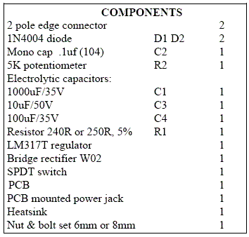
This is a basic,  Universal Power Supply voltage regulator circuit using an LM317, 3-terminal regulator in a TO-220package. The Universal Power Supply output voltage can be set to anywhere in the range one.5V to 30V by selecting resistances. By using a potentiometer, R2, as of the resistors you can dial up the output voltage wanted. Either AC or DC input can be supplied to the PCB by a socket or terminal block. Connection can be either way around. This is because they have provided a bridge rectifier on board. The input DC voltage to the regulator must be at least two.5V above the necessary output voltage. An off/on switch is provided.

For lots of applications (say 12V at 60mA) a heat sink won't be required. The LM317 will provide slightly higher output voltages than 30 volts. However, for most hobbyists over 30V won't be needed. So to make a small PCB they have used some electrolytic capacitors rated to 35 volts. To be safe for continuous operation the maximum input DC voltage to the regulator ought to not be over 33V. With a two.5V to three.0V drop across the regulator this will give a regulated output of 30V. You can draw up to one.5A from the LM317. In case you need higher then use an LM338T rated to 5A.

When outside capacitors are used with any IC regulator it is lovely practice to add protection diodes to prevent the capacitors discharging back in to the regulator in the event of abnormal operating conditions, like a sudden short circuit on the input or the output, or a back emf from an inductive load. That is the function of D one and D Two.

The worth of R1 can range anywhere from 120R to 1200R However, circuits from most other sources settle on using either 220R or 250R. They have used 240R or 250R. The voltage drop across R1is one.25V for all values, and this is the key to the design. one.25V is the reference voltage of the regulator. Whatever current flows through R1 also flows through R2, and the sum of the voltage drops across R1 and R2 is the output voltage. (Additional current Id also flows in R2 but it is usually 50uA so is negligible.)

The design formula are:
VOUT = 1.25 (1 + R2/R1) volts, or alternatively
R2/R1 = (VOUT/1.25) - 1

So in case you know VOUT & R1 is 250R then you can calculate R2. In case you find that the 5K potentiometer used forR2 does not give you the degree of fine control over the voltage output range that you need then you can use these formula to fine-tune R1 & R2 to better suited values.

Universal Power Supply Schematic Diagram

12V DC Switch Mode Power Supply Circuit Diagram

In recent years, the use of switch mode power supply (SMPS) has become more comon as more applications demand for greater power eficiency. It makes use of semiconductor (mostly MOSFET) fast switches to switch DC input that has been rectified at high frequency. The advantages of high frequency switching are that it reduces the size of inductor, capacitors & transformer used. Other advantages of switching power supply over linear power supply are :

1) High Efficiency (up to 90% and above for nice design).
2) Output can be higher than input.
3) Able to operate over a variety of input power supply.
4) Able to have over output.

The setback of using SMPS compared to linear power supply is that it generates electrical noise which contributes to electromagnetic compatibility design issues & more part count.

Buck Converter SMPS
The SMPS circuit below from Power Integration makes use of LNK304 as its high frequency switch. Take note that this circuit is non isolated type which means that the output is not electrically isolated from the input & all testing ought to be completed using an isolation transformer to provide the AC line input to the board.

Make positive that you have electrical safety knowledge & experience before you embark on doing this project.

The features of this project is as summarized below.

Input : 85-265 VAC
Output : 12 V, 120 mA, 1.44 Watt
Low Cost : Only 16 components are needed
No-load power consumption : < 0.2 Watt

12V DC Switch Mode Power Supply (Rise)


Sourced By: Circuitsproject.blogspot.com

Variable DC Power Supply Circuits Diagram

This project provides the schematic & the parts list needed to construct a simple DC Power Supply from an input power supply of 7-20 V AC or 7-30V DC. This project will come in handy in case you use plenty of batteries for your basic electronics project.

Two DC voltage outputs are available; is a fixed regulated 5V for TTL use. The other output is variable from 5V upwards. The maximum output voltage depends on the input voltage. The specified maximum input DC voltage to the regulator is 35V. The maximum input voltage must be two volts higher than the regulated output voltage.

Variable DC Power Supply Circuits Diagram

Variable DC Power Supply Circuits Diagram

The DC Power Supply circuit is based around the 7805 voltage regulator. It's only three connections input, output & ground & it provides a fixed output. The last digits of the part number specify the output voltage, e g. 05, 06, 08, ten, 12,15, 18, or 24. The 7800 series provides up to one amp load current & has on-chip circuitry to close down the regulator if any attempt is made to operate it outside its safe operating area.It can be seen that there's in fact separate circuits in this power supply. 7805 is directly connected as a fixed 5V regulator. The second 7805 has a resistor divider network on the output. A variable 500 ohm potentiometer is used to vary the output voltage from a maximum of 5V up to the maximum DC voltage depending on the input voltage. It will be about 2V below the input DC voltage.

The capacitor across the output improves transient response. The giant capacitor across the input is a filter capacitor to help smooth out ripple in the rectified AC voltage. The larger the filter capacitor the lower the ripple.

For tiny applications the heat sinks won't be needed. The tab on the regulator will dissipate 2W at 25 o C in air. (This is equivalent, for example, to an input voltage of 9V, an output of 5V & drawing 500 m A.) However, as your projects get bigger they will draw more current from the power supply and the regulators will operate at a higher temperature and a heat sink will be needed. You can basically add voltage & current meters to it and put it in to an appropriate plastic case connected to a transformer.

Trouble Shooting Procedure

An LED has been put in to the output of the fixed 5V regulator to indicate that the circuit is working. Poor soldering is the most likely reason that the circuit does not work. Check that all the soldering is done properly. Check that all parts are in their correct position on the PCB. Other items to check are to make sure that the regulators, electrolytic capacitor & bridge rectifier are inserted in the correct orientation.

Variable 5 to 20V DC Supply

If you are looking for a low drop voltage regulator that can provide a power supply of 1A with an output voltage of between 5V and 20V DC, National Semiconductor LM2941 Low Dropout Adjustable Regulator is that you can pick to make use of. It's a typical dropout voltage of 0.5V which means that the input supply need only must be 0.5V DC over the desired output voltage. Its other features include internal short circuit current limit and reverse battery protection.

As shown in the schematic below, the regulator has five pins which consists of the ON/OFF control, Input Voltage, Output Voltage, Ground & Adjustable pins. ON/OFF is used for the purpose of switching on & off of the regulator. The capacitors C1 & E1 are to be placed as close as feasible to the regulator.

The output of the circuit can be varied by varying the worth of potentiometer VR1 from 5V DC to 20V DC. The input voltage is limited from five.5V DC to 30V DC. Resistor R1 must be greater than 1K. The worth of the VR1 that needs to be set is calculated from the formula given below:

VR1 = R1[(Vout/1.275) - 1] ohm

If R1=1K, Vout = 5V, VR1 should be set to 2.9K ohm.

If R1=1K, Vout = 20V, VR1 should be set to 14.7K ohm


5 to 15V Regulated Power Supply

Regulated Power Supply
This project is a normal DC regulated power supply that is a variable DC voltage range from 5V to 15V. It can supply current up to  400mA to power the various circuits for your electronic projects. The voltage output is varied by using the potentiometer V.R1. In this circuit, the input line power supply is designed for 240V.A.C. If 110VAC input is used, alter the ratings of the varistor to 150VAC & the transformer ratio to 110V/12V. 

5 to 15V Regulated Power Supply
Fuse F1 is used as a protection in case there's any short circuit in the circuit. Varistor V1 is connected in parallel to the input of the line voltage to clamp the surge voltage from the line to a reasonable level that helps to protect the transformer & other circuitry. One time the voltage level surge to a high level beyond the ability of the varistor to absorb it, fuse F1 or varistor V1 or both will burn. If this circuit failed after a period of operation, check that the fuse & the varistor are still in nice condition or else replace them.


Diodes D1, D2, D3 and D4 are used to rectify the 12V.A.C voltage to DC voltage. Electrolytic capacitor E1 is used as a smoothing capacitor to reduce the ripple of the DC voltage. The DC voltage is fed in to the input of 7805 regulator where the output DC voltage is obtained. Changing the worth of VR1 will alter the output of the DC voltage. Capacitor C1 is used to filter out high frequency part from the power supply.


2V to 25V Power Supply Schematic

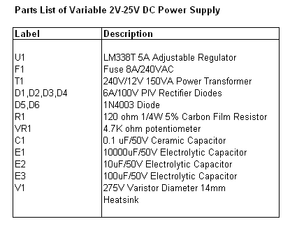
2V to 25 Power supply. This project makes use of a LM338 adjustable three terminal regulator to supply a current of up to 5A over a variable output voltage of 2V to 25V DC. It will come in handy to power up lots of electronic circuits when you are assembling or building any electronic devices. The schematic and parts list are designed for a power supply input of 240VAC. Change the ratings of the parts if 110VAC power supply input is necessary.

2V to 25V Power Supply Schematic

2V to 25V Power Supply Schematic

As shown in the figure above, the mains input is applied to the circuit through fuse F1. The fuse will blow if a current greater than 8A is applied to the method. Varistor V1 is used to clamp down any surge of voltage from the mains to protect the parts from breakdown. Transformer T1 is used to step down the incoming voltage to 24V AC where it is rectified by the diodes D1, D2, D3 & D4. Electrolytic capacitor E1 is used to smoothen the ripple of the rectified DC voltage.

Diodes D5 & D6 are used as a protection devices to prevent capacitors E2 & E3 from discharging through low current points in to the regulator. Capacitor C1 is used to bypass high frequency part from the circuit. Make definite that a large heat sink is mounted to LM338 to transfer the heat generated to the atmosphere.


Simple 50-W Electronic Amplifier Circuit Diagram

This electronic amplifier project is an IC amplifier module from ST Microelectronics, the TDA7294. It is intended for use as a top quality audio class AB amplifier in hi-fi applications. It's low noise and distortion, wide bandwidth and nice output current capability, enabling it to supply high power in to both four ohm and 8 ohm lots. It's both short circuit and thermal protection.

With the addition of a handful of parts and an appropriate power supply, this module will deliver over 50W RMS in to four or 8 ohms-with < 0.1% Total Harmonic Distortion (THD) and < 0.1% Inter-modulation Distortion (IMD). It is also suitable as a replacement power amp stage, or upgrade for plenty of existing amplifiers of between 30W-50W, provided they have an appropriate dual supply, & most do.

The Specifications of the electronic amplifier project there are:

D.C. Input : 35V
Output power : > 50W RMS, 4-8 ohm load.
Gain : 24 dB (30dB modification)
Input sensitivity : one.3V for 50W, 8 ohm
Signal-to-Noise ratio : > 95 dB, (>105 dBA)
Frequency response : approx. 20Hz - 200kHz, �3 dB
Slew rate : > 10V/uS
THD : < 0.01%, 1W-40W, 1kHz
IMD : < 0.01%, 1W

The maximum supply voltage of the IC is +/- 40V. However the maximum dissipation of the IC can be exceeded even at a lower voltage. Therefore the supply voltage used require not be over +/- 35V. This can be constructed using a 50V middle tapped-transformer, a diode bridge rated at 5A (min.) & a pair of electrolytic capacitors, as shown below. A lower secondary voltage transformer could even be used but the reduced DC voltage will lead to less power output in to 8 ohms. You can still receive 50W in to four ohms with only 24V supply rails.

A 36V C.T. transformer will give you approx +/- 25V rails. The-mains transformer used ought to be rated at a maximum of 80VA. In the event you require to run modules in a stereo amplifier you can use a common power supply. In this case the transformer ought to be rated at 150VA or greater.

Electronic Amplifier Circuit Diagram Description

Most of the circuitry is contained within the IC module. The input signal is applied to pin three by capacitor C1 & low-pass filter R1/C2. The filter improves the pulse response & helps cease RF signals. The lower -3dB point is determined-by R2/C1 & R4/C3. This is about 20Hz for the values used. The upper -3dB point is over 200kHz. C7/C8 & C9/C10 provide additional power supply filtering or decoupling.

Simple 50-W Electronic Amplifier Circuit Diagram


R3/R4 are the feedback resistors. The gain is 1+R3/R4 which is approx 16 times, or 24dB. In case you need to increase the input sensitivity you may alter the resistors to suit. Changing R3 to 22k would increase the gain to 30dB and lower the input-required for 50W in to 8 ohm, to 0.6V, without affecting performance much. In case you reduce the worth of R4 you will also need to increase C3 to maintain bass response, as this sets the feedback low frequency roll off.

Pin ten is a mute input and pin 9 provides a standby mode. Muting ought to always happen before standby mode is selected. Connecting these pins permanently to the supply rail ensures that the amplifier comes on immediately on power up. Any switch-on clicks may be eliminated by increasing the time constants of R5/C4 and R6/C5 if necessary.

Make definite that a heavy duty heat-sink rated at least one.4 degree C/W or better is used.

Simple 50-W Electronic Amplifier Circuit Diagram

Sub-Woofer and Controller Circuit Diagram

Sub woofers are popular, with home theater being of the driving forces. However, a nice sub adds considerably to normal hi-fi program material, & so if it is predictable & has nice response characteristics.

 all of sub woofers use a immense speaker driver in a immense box, with tuning vents & all the difficulties (& vagaries) that conventional operation entails. By conventional, I mean that the speaker & cabinet are operated as a resonant technique, using the Thistle-Small parameters to get a box which will (if everything works as it ought to) provide excellent performance.

Completed Prototype


Completed Prototype

A fast word is warranted here, to let you decide if the speaker you have will actually work in a little sealed enclosure. The EAS principle will permit any driver to extend to twenty Hz or even lower. A lovely fast check is to stick the speaker in a box, and drive it to 100W or so at twenty Hz - you ought to see lots of cone movement, a few things will rattle, but you should not actually listen to a tone. A "bad" speaker will generate 60 Hz (third harmonic) - in the event you don't listen to anything, the speaker will work in an equalized sub.

If a tone is audible, or the speaker shows any signs of distress (such as the cone breaking up with appropriate terrible noises), then the driver cannot be used in this manner. Either discover a different driver, or use a vented enclosure.

Before you can build your own EAS box, you will require to pick an appropriate driver, using the above as a guide. Cone tour will be high at the lowest frequencies, so the speaker needs to be able to high power, lovely tour, & of reasonable size (there is no substitute for cone area for moving air at low frequencies). I am using a 380mm (15") driver, but smaller drivers (say 300mm - 12") can be used, or even a bigger number of smaller drivers. I have also had excellent results with a single 300mm driver, which has lower sensitivity (as would expect) but is perfectly adequate for normal usage.


The check methods I used are applicable to any combination, but in general I recommend either a single giant driver or a pair of (say) 300mm units. The next hurdle is the amplifier needed to drive the speaker. This is not trivial. If the selected driver has a sensitivity of 93dB / W @ one metre, then you can safely assume that the efficiency will be less than this below resonance, by a factor of possibly 6dB or more. In case you are used to driving a sub with 100W, this means that you have increased the power to 400W - although this is an over-simplification.

If they are to operate the sub from 60Hz (my aim from the outset), they will increase the power by 12dB for each octave, so if 20W is necessary at 60Hz, then at 30Hz this has increased to 320W, & at 15Hz, you will require over 5kW.

Fortunately, the reality is a tiny different, & 400W or so will be over sufficient for a powerful process, due chiefly to the fact that the energy content in the low bass region is not normally all that great. (Although some program material may have high energy content, in general this is not the case). The EAS process augments the existing process, which is allowed to roll off naturally - contrast this with the normal case, where a crossover is used to separate the low bass from the main process, so existing speaker capability is lost.

The box I built is made from 25mm (1") MDF (Medium Density Fiberboard), & filled with fiberglass. Apart from the fact that it is very heavy (which is a lovely thing, because it desires to walk with low frequencies), the cabinet is acoustically dead, with no resonances in the low frequencies at all ( unlike my house & furniture, dammit !). The woofer is recessed in to the baffle, & sealed with weather sealing foam. When attaching the speaker, do NOT use wood screws, or any other screw in to the MDF. I used "Tee" nuts. I have no idea what they are called elsewhere in the world, but they look like this

TEE NUT

The middle is tapped, and accepts a metal thread screw, and the small spikes mean that you must drill a hole, and hammer in the Tee nut. In case you use a screw through the hole and screwed lightly in to the Tee nut, you can hold it in place as you bash away at it, and can also see that it is straight when you are done. make sure that the finish of the screw doesn't stick out the finish, or you will seldom remove it again after the hammering! I recommend that you lock the tee nut in to place with some construction adhesive (don't get any in the threaded section) so they don't fall out while you are installing the speaker.

The EAS Controller
The controller is (actually very) simple, & the circuit is shown in Figure one. An input buffer ensures that the input impedance of the source does not affect the integrator performance, & allows summing of left & right channels without any crosstalk. The output provides a phase reversal switch, so that the sub can be properly phased to the remainder of the process. If the mid-bass disappears as you advance the level control, then the phase is wrong, so switch to the opposite position.

Figure 1 - The Original EAS Filter / Controller

It turns out that the controller can be simplified, but there is no point. While the dual pot appeared like a lovely suggestion when I built my unit, it actually only changes the gain. Now, having experimented some more, this is an excellent thing, since it means that the level through the controller can be set to make positive that there is no distortion - there can be a immense amount of gain at low frequencies, & if the gain is high, distortion is assured!

The integrators (U1B & U2A) include shelving resistors (R6 & R9), & the capacitor / resistor networks (C1-R4, C3-R7) be positive that signals below 20Hz are attenuated. In case you don't require to go that low, then the worth of the caps (or the resistors R4 & R7) can be reduced. I used four.7uF caps, & these are non-polarized electrolytic - a high value was needed to keep the impedance low to the integrators. I originally included the dual pot (VR1) to permit the upper frequency roll off to be set - however it does no such thing (as described above). The final output level is set with VR2, which may be left out if your power amp has a level control.

It is OK to substitute different op amps, but there is tiny reason to do so. Any substitution tool ought to be a FET input op amp, or DC offset may be an issue. Do not be tempted to make use of a DC coupled amp. If the you are planning to make use of is DC coupled, the input ought to be isolated with a capacitor. Pick a value to give a -3dB frequency of about 10Hz, as this will have tiny effect on the low frequency response, but will help to attenuate the subsonic frequencies.

The unity gain range (using a 20k pot as shown) is from 53Hz to 159Hz. This ought to be sufficient for most systems, but if desired, the resistors (R5 & R8) can be increased in value to 22k, or you can select a bigger value pot. Using 22k resistors & the 20k pot will give a range from 36Hz to 72Hz.

To permit lower frequencies, you can increase the 100k shelving resistors (R6 and R9) to 220k, and increase the high pass capacitors (four.7uF) with 10uF (or R4 & R7 may be increased - a maximum of four.7k is recommended). This will give a turnover frequency of around 8Hz, but expect to make use of much more power, as there will likely be significant sub-sonic energy that will generate huge cone excursions with no audible benefit.

The input must be a standard full range (or for a stampeded method, the whole low frequency signal). Do not use a crossover or other filter before the EAS controller. For final modification, and to integrate the method in to your listening room, I recommend the constant-Q equalizer. The final result using this is extraordinarily nice - I have flat in-room response to 20Hz!

For the power supply, use the in anything else will provide +/-15V at a few Milli amps. My supply is not even regulated, & the whole method is as close to noiseless as you will listen to (or not listen to). Construction is not critical - I built mine on a piece of Overboard (perforated prototype board), & managed to fit everything (including the power supply rectifier & filter) on a piece about 100 x 40 millimeters with room to spare.

The EAS method is surprisingly simple to set up with no instrumentation. Of coursework in case you have an SPL meter & oscillator you can also confirm the settings with measurements. Keep in mind that the room acoustics will play havoc with the results, so unless you require to drag the whole method outside, setting by ear might be the simplest. Even in case you did get it exactly right in an anechoic surroundings, this would alter one time it was in your listening room anyway.

It takes a small experimentation to get right, but is surprisingly simple to do. When properly set, a check track (or bass guitar) ought to be smooth from the highest bass note to the lowest, with no gross peaks or dips. Some are inevitable because of room resonances & the like, but you will discover a setting that sounds "right" with small difficulty.

Performance Of My Prototype
I measured 80dB SPL at one meter in my workshop (sub-woofer perched on a chair in more or less the middle of the space) with at 25Hz & 70W. This improved dramatically when the unit was installed in the listening room, but as I said earlier, there is usually not a lot recorded below around 35Hz. The longest pipe on the organ is usually about 16Hz, but larger pipes still may be used. It was found necessary to cease group of diapasons (able to 8Hz) in the famous Sydney Town Hall organ because when they were used, the very low frequency caused building destroy.

A couple of orchestral recordings revealed traffic (or perhaps underground railway) rumble that I was unaware of before (however this was before it was set correctly, and the bass was a tad louder than needed). One time set up properly, its presence is unobtrusive - except I now have about and a half octaves of additional bottom finish.

I finally decided on a 20Hz maximum frequency (-3dB), and this is reflected in the part values shown in Figure one. The actual roll-over frequency is 16.5Hz, after which the output is attenuated at about 12dB / octave (see Figure two). Without the roll off capacitors, the gain would be 20dB at 20Hz. Unity gain frequencies are about 4Hz and 63Hz with the 20k pot(s) centered.

Figure 2 - Frequency Response of EAS Controller

awesome Australian readers may recognize the woofer brand in the picture (Figure three) of my done unit. The compact size of the box can be seen from the fact that there is tiny spacing around the speaker itself, and most of what is there is the top and sides - I used 25mm MDF, so it makes the outside of the box a bit bigger than the inside. Outside dimensions are 470W x 450H x 410D (18 1/2"W x 17 1/2"H x 16"D), which gives a capacity of 60 liters (about two.1 ft³ - excluding the internal space occupied by the speaker. I think you would agree that this is a small box indeed for a 380mm loudspeaker that performs down to 15Hz.

Figure 3 - Photo of Completed EAS Cabinet


Overall, I would must say that I doubt that any conventional design would be as compact, or would have such clarity & solidarity. Being a sealed box, there is not of the "waffle" that ported designs often give, & the speaker is protected against excessive tour by the air pressure in the box itself (below the cutoff frequency, anyway).

The bottom finish in my technique is now staggering. It is rock solid, & absolutely thunders when called on. The 400W amp is over sufficient for the job, thinking about it's to keep up with a biamped main technique able to high SPL (up to 120dB at my listening position). In fact a fast check indicates that 200W would have been (but \. better to have it & not require it than require it & not have it).

The fact that the EAS design augments the existing speakers than taking over from them with a crossover goes a long way towards ensuring the power requirements do not get out of hand. As an added benefit, I have found that I get the same aural sensation at much lower SPLs - I can listen happily at 90dB, but it sounds much louder. I may even listen to the phone ring while listening now !
All in all, I feel it is unlikely that anything other than an isobaric enclosure could give the same performance for a box size even close to the EAS box,& even then would be limited to about 35Hz. Added to this is the unpredictable combined response of the main speakers and the sub, which is not an Problem with this design. With an EAS system, more power is necessary than a standard design, but for plenty of people, power is less costly than space.

All updates in Your Inbox

Enter your email address:

Delivered by FeedBurner


Copyright @ 2013 Electronic Circuit Diagrams & Schematics.

Designed by AS & AS