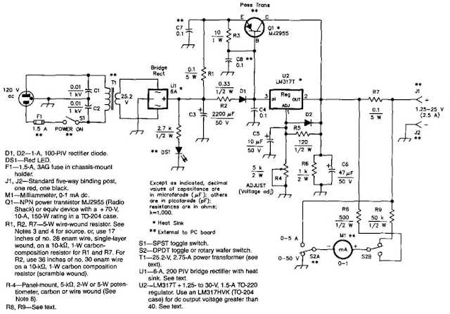
This power supply uses an LM317J adjustable regulator and an MJ2955 pass transistor. Ql and U2 as well as Ul should be heats inked. A suitable heat-sink would typically be 4` 4` 1` fins, extruded type, because up to 65 W dissipation can occur. R8 and R9 should be 1% types or selected from 5% film types with an accurate ohmmeter. Capacitors are disc ceramic except for those with polarity marked, which are electrolytic. D1, D2—1-A, 100-PIV rectifier diode. DS1—Red LED. F1 —1,5-A, 3AG fuse in chassis-mount holder. J1, J2—Standard five-way binding post, one red, one black. M1—Milli-ammeter, 0-1 mA dc. Q1—NPN power transistor MJ2955 (Radio Shack) or equiv device with a + 70-V, 10-A, 150-W rating in a -204 case. R1, R2, R7—5-W wire-wound resistor. See Notes 3 and 4 for source, or, use 17 inches of no. 28 enam wire, single-layer wound, on a 10-KOhmhm, 1-W carbon-composition resistor for R1 and R7. For R2, use 36 inches of no. 30 enam wire on a 10-KOhmhm, 1-W carbon composition resistor (scramble wound). R-4—Panel-mount, 5-kfi, 2-W or 5-W potentiometer, carbon or wire wound (See Note 8). R8, R9—See text. 51—SPST toggle switch. 52—DPDT toggle or rotary wafer switch. T1—25.2-V, 2.75-A power transformer (see text). U1—6-A, 200 PIV bridge rectifier with heat sink. See text. U2—LM317T +1.25- to 30-V, 1.5-A 7-220 regulator. Use an LM317HVK (T0-204 case) for dc output voltage greater than 40. See text.
2.5A-1.25 To 25V Regulated Power Supply Circuit Diagram


0 comments:
Post a Comment