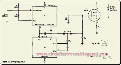
This is a Simple Battery Saving Disconnect Switch Circuit Diagram. At a predetermined level of declining terminal voltage, the circuit disconnects the battery from the load and halts potentially destructive battery discharge. Ql, a high-side, floating-source MOSFET, acts as the switch. The overall circuit draws about 500 when the switch is closed and about 8 when it`s open.
Battery Saving Disconnect Switch Circuit Diagram
The values of ii, R2, and R3 set the upper and lower voltage thresholds, Vv and VL, according to the relationships For the circuit to start, V+ must exceed VO. The voltage detector IC1 then powers IC2, but only while V+ remains above VL. Otherwise, IC2 loses its power, removes gate drive from Ql, and turns it off. IC2 is a dual chaige-pump inverter that normally converts 5 V to + 10 V. Capacitors CI, C2, and the two associated diodes form a voltage tripler that generates a gate drive for Ql that is approximately equal to two times the battery voltage.
With the values in the schematic, the circuit disconnects 3-cell Nicad battery from its load when V+ reaches a VL of 3.1 V. Approximately 0.5 V of hysteresis prevents the switch from turning on immediately when the circuit removes the load; V+ must first return to Vu, which is 3.6 V. The gate drive declines as the battery voltage declines, cause the ON-resistance of Ql to reach a maximum of approximately 0.1, just before V+ reaches its 3.1-V threshold. A 300-mA load current at that time will cause a 30-mV drop across the disconnect switch. The drop will be 2 to 3 mV less for higher battery voltages. Resistor R4 ensures that Ql can adequately turn off by providing a discharge path for C2.


0 comments:
Post a Comment